Quantum and 2D Metamaterials
Our research
Quantum metamaterials
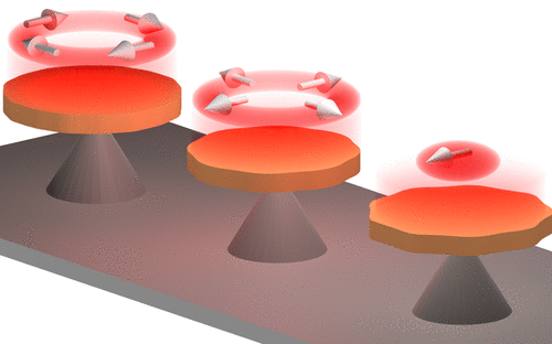
As with a conventional metamaterial, a quantum metamaterial is composed of an array of resonant meta-atoms at a scale comparable to, or smaller, than the wavelength of interest. What sets quantum metamaterials apart is that the behaviour of these individual building blocks, and therefore the overall response of the metamaterial, is determined by laws of quantum mechanics. There is an extensive list of potential meta-atoms to explore, such as semiconductor quantum dots, solid-state defects, superconducting qubits, and cold atoms. The challenge lies in manufacturing and controlling large scale arrays, whilst maintaining quantum coherence across the ensemble.
If this control can be realised, quantum metamaterials offer enticing long-term opportunities in the processing, storage and networking of quantum information, and in nearer-term applications, such as solar energy harvesting and quantum-enhanced sensing and imaging.
Our research
Our work is focused on the development of meta-atoms and their integration into quantum metamaterials, as well as new devices and materials for applications in quantum technology.
We investigate:
- Meta-atoms, including Solid-state defects and semiconductor quantum dots,
- 2D-material heterostructure engineering,
- Novel materials and devices for the generation and detection of quantum light,
- Integrated devices for quantum sensing,
- Quantum enhanced imaging,
- Theory of quantum metamaterials and quantum information processing.
2D metamaterials
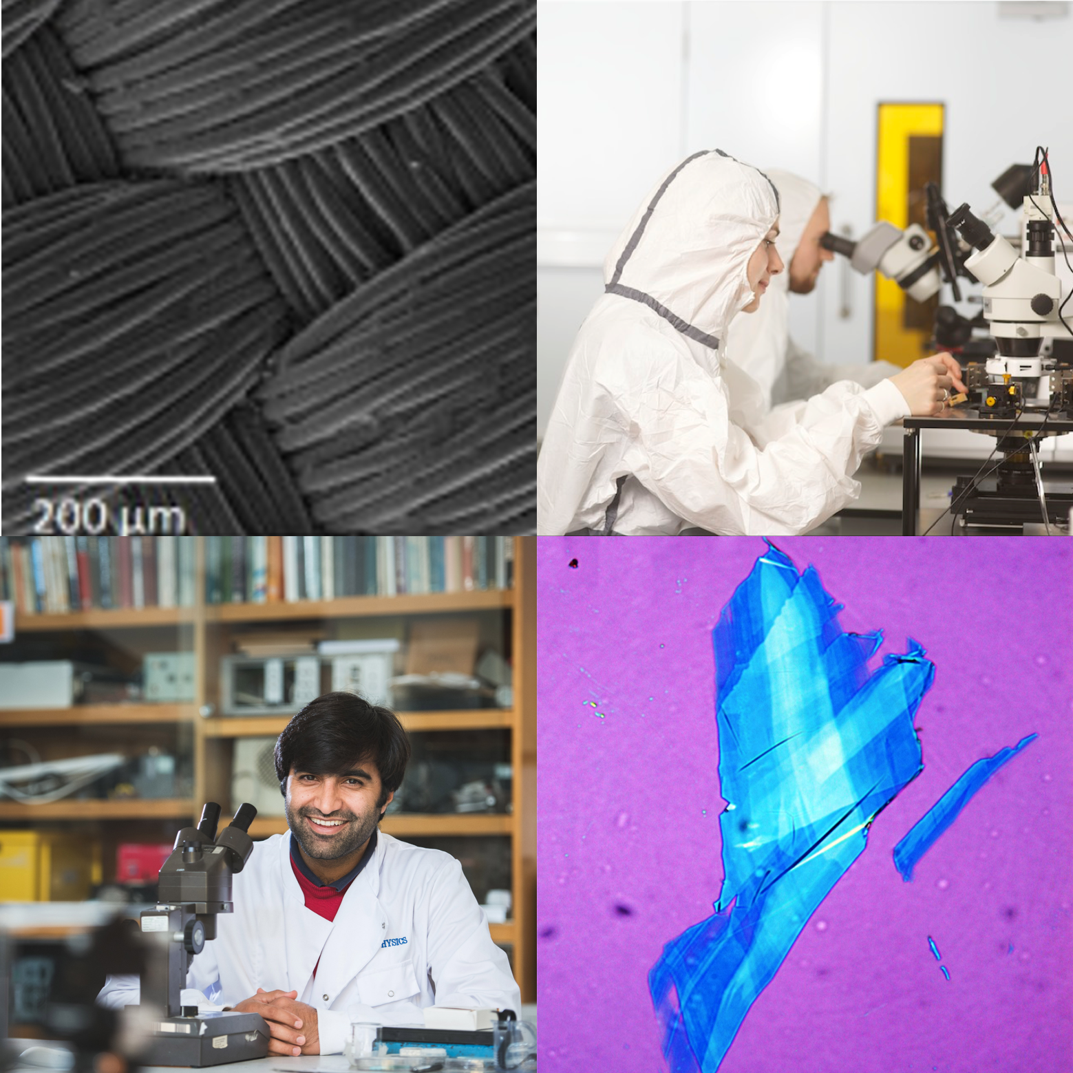
The synthesis of 2D materials, with thicknesses of only a few atoms, has ushered in an exciting new era for materials science. The reduced dimensionality of these materials, such as graphene or hexagonal boron nitride, leads to incredible electronic, mechanical, photonic and thermal properties such as huge electrical & thermal conductivities, optical transparency and impressive mechanical flexibility. Combining 2D materials into heterostructures produces even more possibilities by tailoring the van der Waals interaction between layers.
The extraordinary properties of 2D materials and their heterostructures make them a natural choice as building blocks in metamaterial systems that can display properties unseen in the natural world.
Our research
The research in the CMRI on 2D metamaterials encompasses the entire scope with computation & theory to predict the properties of materials and heterostructures, fabrication & lithography of the samples and the measurement of properties. Some of the research directions our inter-disciplinary team are pursuing in this area include:
- Electrical tuning of 2D interlayer excitons,
- Single photon detection and emission,
- Predicting the structure of 2D materials and interfaces in heterostructures,
- Novel quantum phenomena in nanoelectronics,
- Integration of 2D materials with textiles.
Real-world applications
Metamaterials composed of 2D materials represent an exciting prospect for a variety of applications, some of the practical developments that we have already been working towards include:
- Wearable self-powered biosensors using 2D materials on textiles,
- Ultra-thin and flexible environmental sensors (measuring pressure, humidity and temperature),
- Coatings to improve the efficiency of solar panels.
In addition to these areas, our researchers are always keen to explore new ways at bridging the gap between scientific development and industrial applications.
Alex Savchenko Centre for Nanoscience
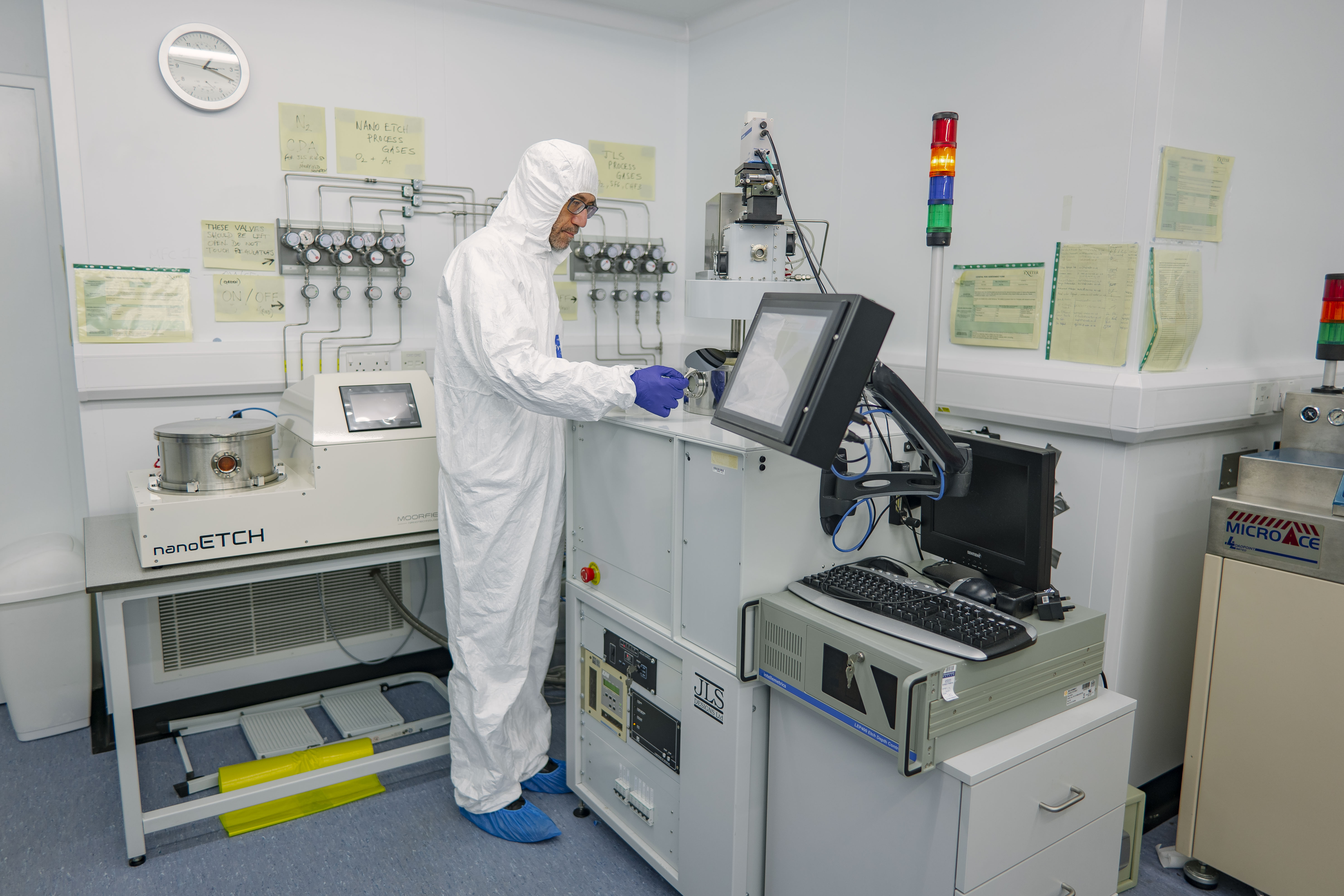
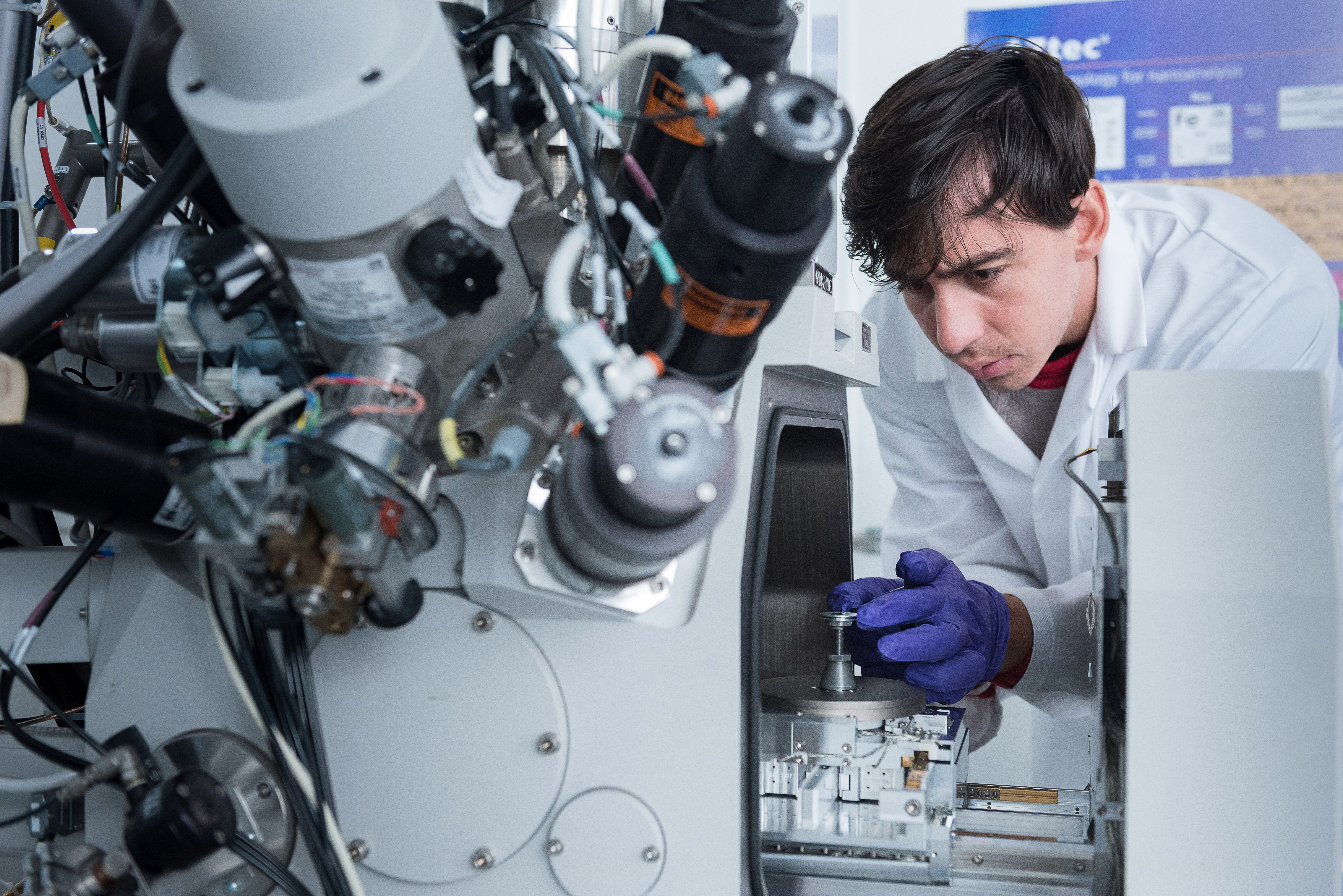
We have two cleanrooms covering a total of 150 m2. The Savchenko Centre is a purpose built semiconductor type cleanroom with advanced air-condition control of temperature and humidity to provide ISO Class 5 and 6 working environments. An acid bench with an integrated DI water system and two solvent benches, all with their own Class 4 laminar air flow systems, are built into the facility to complement the fabrication process.
A second cleanroom is used as a dedicated optical lithography area housing a number of optical lithography and deposition systems.
Optical Lithography
- NanoBeam NB4 Electron Beam System,
- Durham Magneto Optics MicroWrite ML laser writer
- Karl Suss MJB4 Optical Mask Aligner,
- and Kloe UV-Kub 2 masking optical system.
Deposition Systems
- Kurt J Lesker Evaporation System,
- HHV Auto306 Thermal Evaporator,
- and Moorfield nanoPVD S10A sputtering system.
Processing Systems
- JLS Designs RIE 80 Etching System,
- Moorfield Nano ETCH,
- LoadPoint Micro Ace 3 Dicing Saw,
- K&S 4123 and 4700 Wire Bonders,
- and Critical Point Drier.
Our researchers in this area include:
 |
 |
 |
| Dr Changxu Liu | Prof Euan Hendry | Dr Isaac Luxmoore |
 |
 |
 |
| Dr Maciej Dabrowski | Prof Monica Craciun | Prof Saverio Russo |
 |
||
| Dr Steve Hepplestone |


